Two day workshop on VLSI Design in GNDEC
Author(s): City Air NewsGathering during two-day workshop on VLSI Design held in GNDEC, Ludhiana. Ludhiana, October 14, 2015: IETE Student forum, Department of Electronics and Communication Engineering, Guru Nanak Dev Engineering College,...
 cityairnews
Oct 14, 2015 12:30
0
cityairnews
Oct 14, 2015 12:30
0


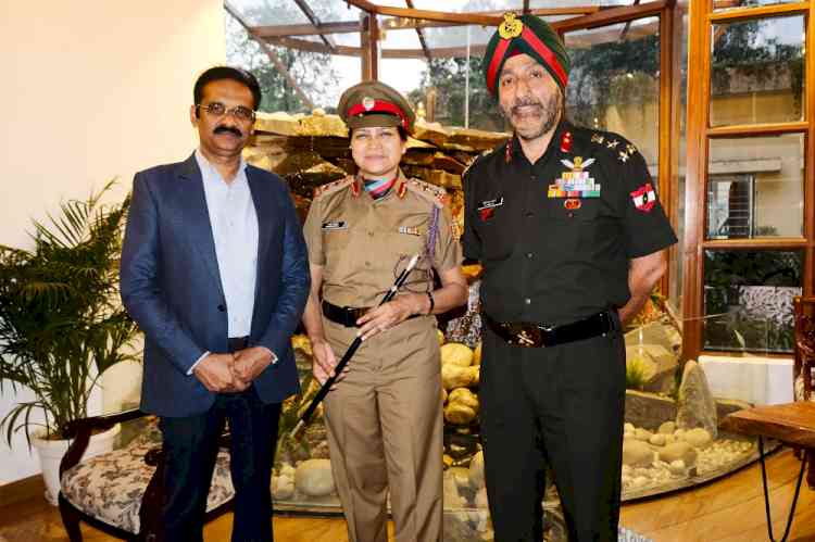
Gathering during two-day workshop on VLSI Design held in GNDEC, Ludhiana.
Ludhiana, October 14, 2015: IETE Student forum, Department of Electronics and Communication Engineering, Guru Nanak Dev Engineering College, Ludhiana has organised a two day workshop on VLSI Design. The prime intent behind this event is to incite passion amongst participants to take career in most exciting field of Engineering – Space Technology and Microelectronics. Also, it will proffer a brief framework about Integrated Circuit Design.
Scientists from SCL, Department of Space, Govt. of India, Sh. H. S. Jatana and Sh. Munish Malik were invited to present their expertise on Integrated circuit Design. The guests were welcomed by Dr. M.S Saini, Director GNDEC. On this ocassion,Dr. S. S. Gill, HOD, ECE Deptt., GNDEC said that the workshop is being conducted under the recently signed MoU between the two organisations for enhancing R&D activities in the field of VLSI among students and the teaching fraternity.
Sh. H. S. Jatana in his address said that SCL is the only facility of its kind in India and this workshop will galvanize VLSI research and knowledge among the faculty and students. Also, it will help in filling the gap between institute and industry by providing an industry focussed shape to classroom sessions.
Date:
Wednesday, October 14, 2015